Section 1: Analogue and Digital Signals
Electronic circuits process electrical signals. A signal is a voltage that carries information — it tells the circuit when to switch on or off, or what value something is. There are two fundamentally different types of signal:
Analogue signals
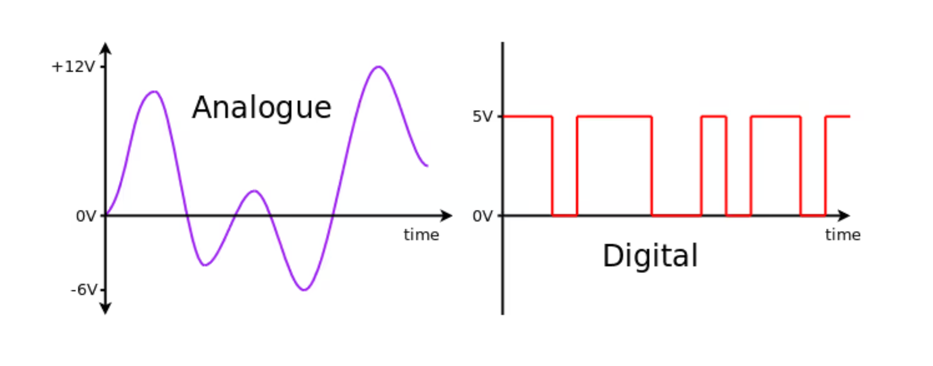
An analogue signal can be any voltage value between a minimum and maximum. It changes smoothly and continuously, like a dimmer switch or a volume control. A good example is the light level outside — it gradually gets brighter from dawn, reaches a peak at midday, and slowly fades to dark.
Digital signals
A digital signal can only be one of two values — ON or OFF. In electronics, these are represented as:
A simple switch is a digital input — it is either open (0) or closed (1). There is no in-between. All computers, smartphones and digital systems work entirely with 1s and 0s.
Section 2: Logic Gates
A logic gate is an electronic component that takes one or more digital inputs and produces a single digital output. The output depends entirely on the combination of inputs — and that relationship is described precisely using a truth table and a Boolean expression.
Logic gates are the building blocks of all digital systems — from simple alarm circuits to the billions of transistors inside a modern CPU (Central Processing Unit — the "brains" of a computer, which executes instructions and processes information).
The NOT gate (Inverter)
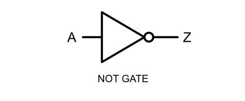
The NOT gate has one input and one output. It simply inverts the input — if the input is 1, the output is 0, and vice versa. The small circle (bubble) on the output of the symbol represents inversion.
TRUTH TABLE
| Input A | Output Z |
|---|---|
| 0 | 1 |
| 1 | 0 |
A truth table lists every possible combination of inputs a gate can have, and shows the output that results for each one. This lets us describe exactly how a gate behaves, with no ambiguity — once you know a gate's truth table, you know everything about how it works.
Real-world example: A NOT gate is needed in a burglar alarm when a light beam is used. Light shines onto a sensor which gives a logic 1 output (beam intact = safe). When a burglar breaks the beam, the sensor output is turned off (logic 0). So a NOT gate is used to invert the signal. This enables a logic 1 signal to trigger an alarm.
The AND gate
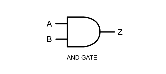
The AND gate has two (or more) inputs and one output. The output is only logic 1 when ALL inputs are logic 1 simultaneously. If any input is 0, the output is 0.
TRUTH TABLE
| Input A | Input B | Output Z |
|---|---|---|
| 0 | 0 | 0 |
| 0 | 1 | 0 |
| 1 | 0 | 0 |
| 1 | 1 | 1 |
Real-world example: A safety press on a machine — both the operator's left hand button (A) AND right hand button (B) must be pressed before the machine operates. This prevents the operator from accidentally putting a hand under the press.
The OR gate
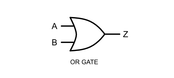
The OR gate has two (or more) inputs and one output. The output is logic 1 when ANY input is logic 1. The output is only 0 when all inputs are 0.
TRUTH TABLE
| Input A | Input B | Output Z |
|---|---|---|
| 0 | 0 | 0 |
| 0 | 1 | 1 |
| 1 | 0 | 1 |
| 1 | 1 | 1 |
Real-world example: The courtesy light in a car. Input A: the driver's door is opened. Input B: the passenger's door is opened. Output: the interior roof light turns on. This is useful because you need the light to come on so you can see inside the car, regardless of which door is used to get in.
| Input A | Input B | Output Z |
|---|---|---|
| 0 | 0 | |
| 0 | 1 | |
| 1 | 0 | |
| 1 | 1 |
Section 3: Combinational Logic Circuits
When two or more logic gates are connected together to perform a specific task, the result is called a combinational logic circuit. The output depends on the combination of all current inputs.
How many rows in a truth table?
The number of rows in a truth table doubles with each additional input:
| Number of inputs | Number of rows |
|---|---|
| 1 | 2 |
| 2 | 4 |
| 3 | 8 |
| 4 | 16 |
Just as each column in a decimal number represents a power of 10 (units, tens, hundreds...), each column in a binary number represents a power of 2. Reading from the right: the 1s column, then the 2s column, then 4s, then 8s — each column worth double the one before it.
There's a standard pattern to how the columns fill in as you count: the right-most column alternates every row (0, 1, 0, 1...), the column to its left alternates every 2 rows, the column after that every 4 rows, and so on. Each column added to the left doubles the pattern length — 2, 4, 8, 16, 32, 64, 128, 256, 512, 1024... These are the same numbers you'll recognise from phone, computer and flash drive storage sizes — it's all built on the same binary counting system.
Here's decimal 0–15 built up from those column values:
| Decimal | 8s | 4s | 2s | 1s | Binary |
|---|---|---|---|---|---|
| 0 | 0 | 0 | 0 | 0 | 0000 |
| 1 | 0 | 0 | 0 | 1 | 0001 |
| 2 | 0 | 0 | 1 | 0 | 0010 |
| 3 | 0 | 0 | 1 | 1 | 0011 |
| 4 | 0 | 1 | 0 | 0 | 0100 |
| 5 | 0 | 1 | 0 | 1 | 0101 |
| 6 | 0 | 1 | 1 | 0 | 0110 |
| 7 | 0 | 1 | 1 | 1 | 0111 |
| 8 | 1 | 0 | 0 | 0 | 1000 |
| 9 | 1 | 0 | 0 | 1 | 1001 |
| 10 | 1 | 0 | 1 | 0 | 1010 |
| 11 | 1 | 0 | 1 | 1 | 1011 |
| 12 | 1 | 1 | 0 | 0 | 1100 |
| 13 | 1 | 1 | 0 | 1 | 1101 |
| 14 | 1 | 1 | 1 | 0 | 1110 |
| 15 | 1 | 1 | 1 | 1 | 1111 |
Method for completing a truth table from a circuit
Label the output of each intermediate gate with a letter (D, E, F etc.). Then fill in one column at a time, working left to right through the circuit.
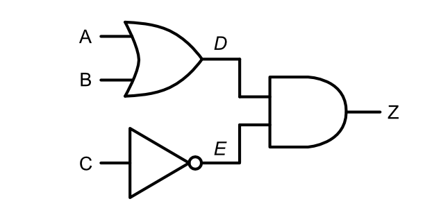
Circuit: A and B feed an OR gate (output D). C feeds a NOT gate (output E). D and E feed an AND gate (output Z).
| A | B | C | D (A OR B) | E (NOT C) | Z (D AND E) |
|---|---|---|---|---|---|
| 0 | 0 | 0 | 0 | 1 | 0 |
| 0 | 0 | 1 | 0 | 0 | 0 |
| 0 | 1 | 0 | 1 | 1 | 1 |
| 0 | 1 | 1 | 1 | 0 | 0 |
| 1 | 0 | 0 | 1 | 1 | 1 |
| 1 | 0 | 1 | 1 | 0 | 0 |
| 1 | 1 | 0 | 1 | 1 | 1 |
| 1 | 1 | 1 | 1 | 0 | 0 |
For each circuit, complete the truth table by filling in the intermediate gate outputs and the final output. Check your answers using the NoNANDSense simulator.
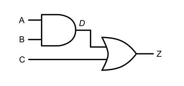
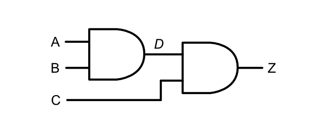
| A | B | C | D (A AND B) | Z (D OR C) |
|---|---|---|---|---|
| 0 | 0 | 0 | ||
| 0 | 0 | 1 | ||
| 0 | 1 | 0 | ||
| 0 | 1 | 1 | ||
| 1 | 0 | 0 | ||
| 1 | 0 | 1 | ||
| 1 | 1 | 0 | ||
| 1 | 1 | 1 |
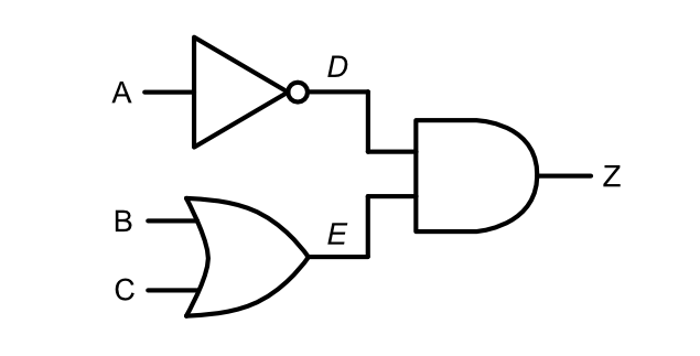
| A | B | C | D (NOT A) | E (B OR C) | Z (D AND E) |
|---|---|---|---|---|---|
| 0 | 0 | 0 | |||
| 0 | 0 | 1 | |||
| 0 | 1 | 0 | |||
| 0 | 1 | 1 | |||
| 1 | 0 | 0 | |||
| 1 | 0 | 1 | |||
| 1 | 1 | 0 | |||
| 1 | 1 | 1 |
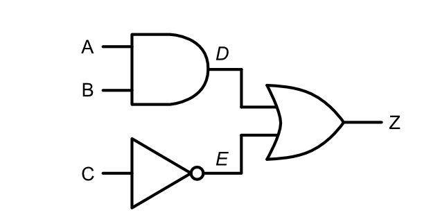
| A | B | C | D (A AND B) | E (NOT C) | Z (D OR E) |
|---|---|---|---|---|---|
| 0 | 0 | 0 | |||
| 0 | 0 | 1 | |||
| 0 | 1 | 0 | |||
| 0 | 1 | 1 | |||
| 1 | 0 | 0 | |||
| 1 | 0 | 1 | |||
| 1 | 1 | 0 | |||
| 1 | 1 | 1 |
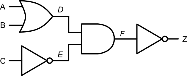
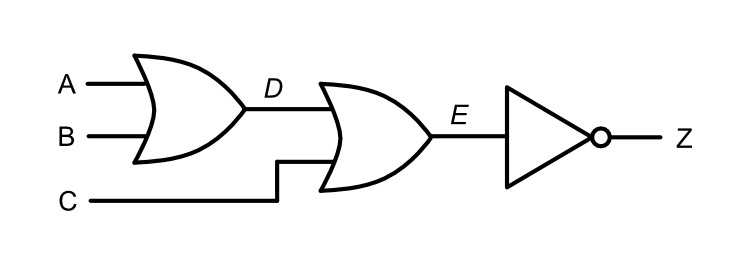
| A | B | C | D (A OR B) | E (NOT C) | F (D AND E) | Z (NOT F) |
|---|---|---|---|---|---|---|
| 0 | 0 | 0 | ||||
| 0 | 0 | 1 | ||||
| 0 | 1 | 0 | ||||
| 0 | 1 | 1 | ||||
| 1 | 0 | 0 | ||||
| 1 | 0 | 1 | ||||
| 1 | 1 | 0 | ||||
| 1 | 1 | 1 |
Section 4: Boolean Algebra
Boolean algebra was developed by the British mathematician George Boole in the 1850s. It gives us a precise mathematical language to describe the behaviour of logic circuits. Today it is used by every electronic engineer, computer scientist and software developer.
Boolean notation summary
| Gate | Symbol | Meaning | Example | |
|---|---|---|---|---|
|
A | NOT A | Z = A | Z is ON when A is OFF |
|
. | AND | Z = A.B | Z is ON when A AND B are ON |
|
+ | OR | Z = A+B | Z is ON when A OR B (or both) are ON |
Single-gate examples
Before combining gates together, make sure you're comfortable writing the Boolean expression for a single gate on its own.
Writing a Boolean expression from a circuit
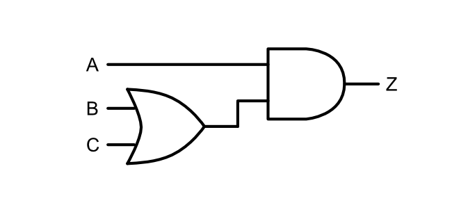
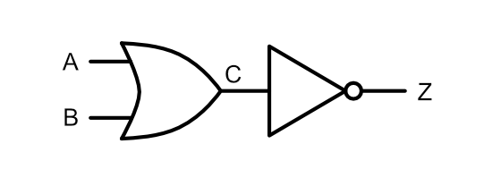
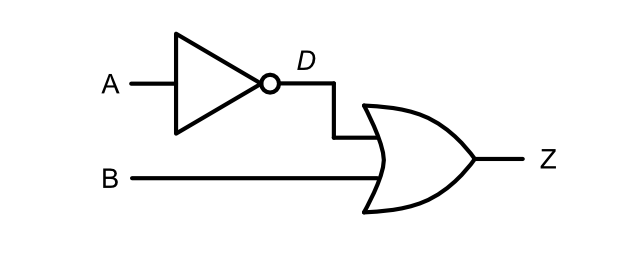
Work through the circuit left to right, writing an expression after each gate. Bracket sub-expressions where needed.
From circuit to truth table
Once you've labelled the intermediate points in a circuit, you can use those labels to build up a truth table one column at a time — just like the worked example below. Try it for the circuit where A and B feed an OR gate, and the OR output together with C feed an AND gate:
| A | B | C | (A+B) | (A+B).C |
|---|---|---|---|---|
| 0 | 0 | 0 | ||
| 0 | 0 | 1 | ||
| 0 | 1 | 0 | ||
| 0 | 1 | 1 | ||
| 1 | 0 | 0 | ||
| 1 | 0 | 1 | ||
| 1 | 1 | 0 | ||
| 1 | 1 | 1 |
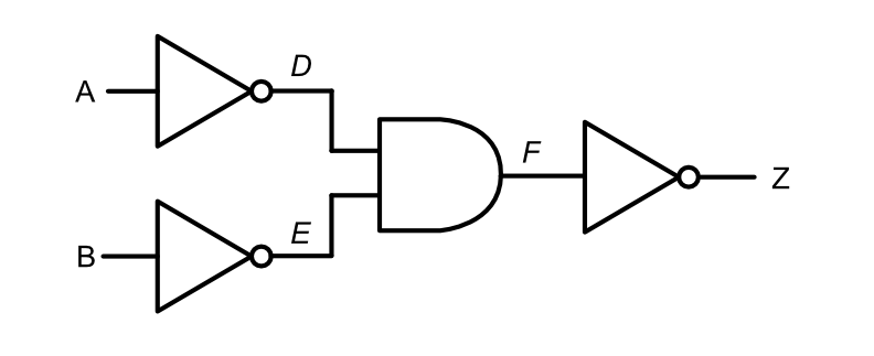
For each circuit below, complete a truth table and write the Boolean expression for Z.
Section 5: Boolean Expressions from Truth Tables
Sometimes you will be given a truth table and asked to write the Boolean expression and draw the circuit. The method is straightforward — focus only on the rows where the output is logic 1.
Method
- Look at the truth table and highlight every row where Z = 1
- For each highlighted row, write an AND expression for that combination of inputs. If an input is 0, write its complement (with a bar): e.g. A. If it is 1, write it normally: A.
- Connect all the row expressions with OR (+) to get the full Boolean expression
- Draw the logic circuit from the expression
Truth table with 3 inputs A, B, C and output Z:
| A | B | C | Z |
|---|---|---|---|
| 0 | 0 | 0 | 0 |
| 0 | 0 | 1 | 0 |
| 0 | 1 | 0 | 1 |
| 0 | 1 | 1 | 0 |
| 1 | 0 | 0 | 1 |
| 1 | 0 | 1 | 0 |
| 1 | 1 | 0 | 0 |
| 1 | 1 | 1 | 0 |
For each truth table, write the Boolean expression for Z. Then build and verify the circuit using NoNANDSense.
| A | B | Z |
|---|---|---|
| 0 | 0 | 0 |
| 0 | 1 | 1 |
| 1 | 0 | 0 |
| 1 | 1 | 0 |
| A | B | Z |
|---|---|---|
| 0 | 0 | 1 |
| 0 | 1 | 0 |
| 1 | 0 | 1 |
| 1 | 1 | 0 |
| A | B | C | Z |
|---|---|---|---|
| 0 | 0 | 0 | 0 |
| 0 | 0 | 1 | 0 |
| 0 | 1 | 0 | 0 |
| 0 | 1 | 1 | 0 |
| 1 | 0 | 0 | 0 |
| 1 | 0 | 1 | 1 |
| 1 | 1 | 0 | 0 |
| 1 | 1 | 1 | 1 |
Section 6: Designing Circuits from a Specification
The most common engineering application of digital logic is designing a circuit to meet a given written specification. Read the specification carefully — the key words AND, OR and NOT tell you which gates are needed.
Method
- Identify all the inputs from the specification
- Identify the output
- Read the specification and identify the logic: look for AND, OR, NOT
- Write the Boolean expression
- Draw the logic circuit
- Draw up the truth table (all input combinations)
- Verify using the simulator
"A burglar alarm should sound if the master switch is on AND either a light beam is broken OR a pressure pad is triggered."
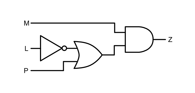
| M | L | P | L | L+P | B (alarm) |
|---|---|---|---|---|---|
| 0 | 0 | 0 | 1 | 1 | 0 |
| 0 | 0 | 1 | 1 | 1 | 0 |
| 0 | 1 | 0 | 0 | 0 | 0 |
| 0 | 1 | 1 | 0 | 1 | 0 |
| 1 | 0 | 0 | 1 | 1 | 1 |
| 1 | 0 | 1 | 1 | 1 | 1 |
| 1 | 1 | 0 | 0 | 0 | 0 |
| 1 | 1 | 1 | 0 | 1 | 1 |
For each specification: identify inputs and outputs, write the Boolean expression, draw the circuit diagram and complete the truth table. Verify using NoNANDSense.
Section 7: Logic Gate Integrated Circuits (ICs)
In practice, logic gates are not individual components — they are built into integrated circuits (ICs), also called chips. Each IC contains several logic gates in a single small package.
The chips used in school are TTL (Transistor-Transistor Logic) chips, which require a stable +5V supply. The chip number always starts with 74:
| IC number | Contents | Description |
|---|---|---|
| 7404 | 6 × NOT gates | Hex inverter — six independent NOT gates |
| 7408 | 4 × 2-input AND gates | Quad 2-input AND |
| 7432 | 4 × 2-input OR gates | Quad 2-input OR |
All three chips use the same 14-pin layout principle — Vcc on pin 14, GND on pin 7, with the gates arranged around the remaining pins:
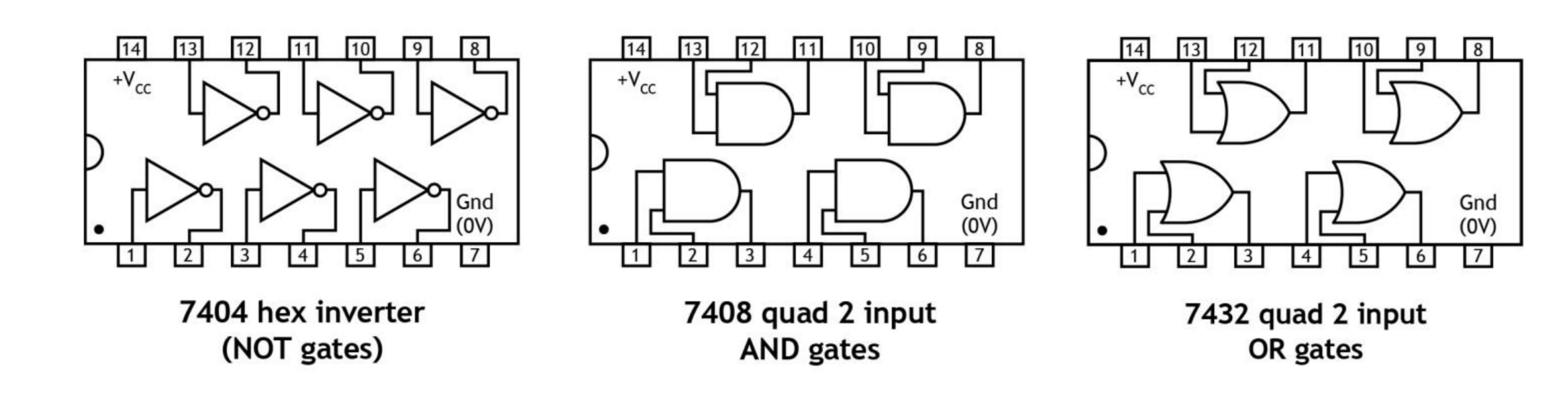
The NoNANDSense IC diagram feature
The NoNANDSense simulator includes a 7400 Series Circuit Diagram tool. After building your logic circuit, this tool automatically selects the correct IC chips, groups gates into ICs, and draws the physical wiring diagram — ready for building on a breadboard.
Section 8: Real-World Applications of Logic Gates
Logic gates are found in almost every electronic system. Understanding how they work allows engineers to design control systems, safety systems, automation and more.